During quarantine, I found some fantastic videos by Ben Eater walking through the process of building an 8-bit CPU on breadboards. This was based on a simple CPU design outlined in Digital Computer Electronics. Getting the basic CPU up and running was a lot of fun, but I wanted to go further and make the CPU more capable. In this post, I’ll share some tips on building and upgrade to 256 bytes of single port RAM, expand all the registers to a full 8 bits, and improve the microcode to add more instruction steps and a reset microcode.
This is the first part of a two-part series. Once you’re done, make sure to read part two where I add a stack pointer, Arduino programming, and more control lines.
General Tips
I want to call out some great resources available from the Reddit community:
For those who are new to electronics, I highly recommend two things: a cheap oscilloscope and bench power supply. You can certainly do without them, but I think they can really reduce frustration. Here’s some general tips:
- Oscilloscope: I think that the direct visual representation of an oscilloscope vs. a multimeter or having to constantly probe with LEDs makes it much, much easier to understand what’s going on. Especially if you’re new to electronics! You can get a Siglent DSO5102P which costs $240 on Amazon and will be more than enough for not just this project, but many electronics projects you’ll encounter down the road.
- Power Supply: You can use Ben’s power supply, but a proper power supply will come in handy because it’ll protect you from mistakes and ensure you can always give it enough juice. Again, this is important if you’re new to electronics! Just set the current limiter slightly above what your normal draw is and you’ll easily be able to tell if you’ve shorted something without damaging your components. You can get this Eventek KPS305D for $55 on Amazon which supports 30V/5A and it’ll work just fine.
- Logic Analyzer/Multimeter: I didn’t really use these during the build as I found them completely unnecessary. If you just want to play with a logic analyzer (may be better with the 6502 build), the HiLetgo 8 Channel USB analyzer is $13 on Amazon and supports PulseView. You’ll also want to get some breadboard jumper ribbon cables, which are $6 on Amazon.
- Power and Ground: Try to connect all your power rails as much as possible so current can flow freely. Beyond power running down each side, make sure to connect the two “halves” of your CPU with wires bridging across the bus, for each power rail. Check your voltages at the far end to make sure they’re not dropping too much and that your ground is the same throughout!
- Capacitors: I know everyone talks about it, but I’ll just reiterate that this is really critical to not getting random bugs that drive you crazy and are impossible to figure out. Some people think the “bigger the better” but the capacitor value and type needs to match the kind of noise you’re expecting, so you need to be specific. Here’s a recommendation:
- 0.1 uF: Put a couple of 0.1uF capacitors on each breadboard’s power rail (ideally 1 per chip), as close to each chip’s power/ground wires as possible. These are usually orange and marked “104” on the side.
- 1 uF: Put one 1uF electrolytic capacitor on each breadboard’s power rail, near where the power/ground wires enter your breadboard. These are usually black and cylindrical and they only go in one direction (there’s a white line denoting the negative terminal).
- 10 uF: Put 1-2 big electrolytic capacitors (10uF) near where the power supply connects and then at the far end of your board. Like their 1 uF counterparts, these are usually black and cylindrical and only go in one direction.
- LEDs: Don’t forget that LEDs only work in one direction (the negative side has the shorter leg and has a notch on the base). Be disciplined about putting resistors on LEDs or you risk not just burning out the LED but weird problems. During one part of my build, I was lazy and decided to put some on later but they actually caused random behavior with some of the chips. I only realized my mistake after wasting a good hour of debugging!
- Soldering: I find it much easier to solder resistors directly to LEDs. It helps tell the direction of the LED and it’s easier to fit on the board. You just take the leg of the resistor and the leg of the LED, twist them together with some pliers, and then add a bit of solder. If you’re new to soldering, here’s what you need to know:
- Soldering Iron: These days you don’t need to spend a lot of money to get a great iron. The TS100 is one of the best irons available and it’s $70 on Amazon. If you’re new to soldering, get the BC2 tip because it’s easier to get more heat transferred with the flat side. As you gain more experience and maybe get into SMT, you may want to explore other tips. Upgrade to open-source firmware to improve the iron for free.
- Solder and Tools: If you’re a beginner, use 63/37 leaded solder. Don’t use non-leaded and don’t use 60/40 (because it’s not eutectic) if you’re just starting out because they require more skill. Once you get the hang of things, you can switch if you’re concerned about environmental/health effects. You can get an anti-static soldering mat and multi-arm station (with fan) to help make things easier, but it’s not necessary.
- Debugging: The key thing about circuits is they always do exactly what you tell them. It’s just that, sometimes you don’t know what you’re telling them. The key to debugging effectively is to isolate the problem and try to get it down to a few possibilities. Don’t just assume certain things are happening, make sure! Use the principle of deduction to narrow down problems. If it’s the 7th bit, you know the issue is with the upper chip. If it’s happening during only one state, isolate your signals from the system and manually drive the chip to see what’s going on. Don’t trust that your wires are well-connected, don’t trust your power/ground, and don’t trust your LEDs. Always check!
- Learning More (Art of Electronics): If you want to learn more about these topics and practical electronics in general, the Art of Electronics is probably the greatest practical reference written about the subject. While it looks like an academic textbook, it’s extremely approachable and deals with only practical questions about electronics. It’s an invaluable resource for Ben’s build and anything you may do in the future.
Parts List
To expand the RAM, you’ll need:
- 1x Cypress CY7C199 (Jameco, Datasheet) which has 32K bytes of RAM. Something like 62256 would also work. At the end of this, we’ll only be able to address 256 bytes but it gives flexibility for future expansion.
- 1x 74LS161 (Jameco, Datasheet) which is a 2nd counter chip to make the program counter 8-bit.
- 1x 74LS173 (Jameco, Datasheet) which is a 2nd register chip to make the memory address register 8-bit.
- 1x 74LS32 (Jameco, Datasheet) which is an OR Gate which we’ll need for some signals.
- 13x 1K Resistors (Jameco) to use as pulldowns/pullups for signaling.
- 1x 8-bit DIP switch to program the longer addresses.
- 4x Yellow LEDs, 7x Green LEDs, 11x 220 Ohm resistors to expand the address register (yellow), program counter (green), and t-state counter (green). If you want, you can replace the instruction register LEDs to be the same color since it’ll just be one 8-bit opcode.
We will reuse the 74LS245 (bus transceiver), 74LS157 (2-input mux), 74LS04 (inverter) from the existing build.
Step 1: Upgrade the RAM
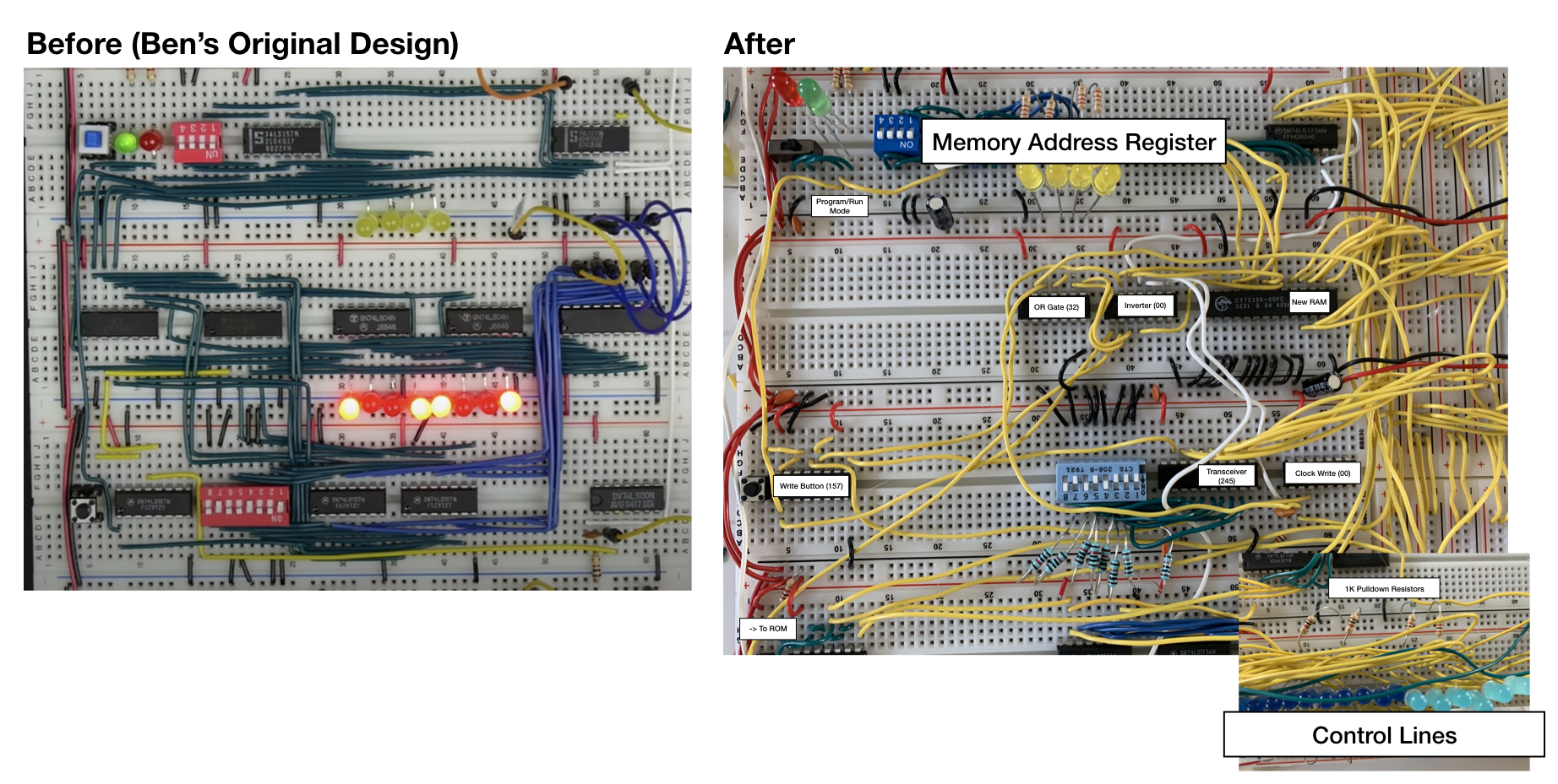
Adding the RAM
Since everything else depends on the RAM, we’ll start there. In order to make sure everything is working well, we’ll integrate the RAM into the existing 4-bit system before moving to the next step. Let’s first hook up the RAM to the bus:
- Remove the 74LS245, the two 74189s, the two 74LS157s next to the 8-bit DIP switch, the 8-bit DIP switch, and the two 74LS04s that inverted the RAM output. Make sure to keep the clock-based write circuit (74LS00) and the button-based write circuit (74LS157)!
- You should now have an empty breadboard where the RAM was and more space where you used to program the RAM. Your memory address register and memory DIP switch should remain as-is.
- Put the CY7C199 next to the bus (where the 245 used to be) and put a 74LS04 and 74LS32 next to it. Wire the chips all up to power and ground.
- Take the four address lines from the memory address register and wire them to A0 - A3 on the top side of the RAM. For now, wire A4 - A14 to ground.
- Wire IO0 - IO7 on the RAM directly to the bus.
- Test that the RAM is working by setting Counter Out high (so your bus isn’t driven by the program counter) and connecting WE to power, OE to ground, and CE to ground. Toggle the address lines and observe that random stuff is showing on the bus. Success!
Adding the DIP Switch Writer
So now that we know the RAM is outputting onto the bus, how do we write to it? We’ll use a different method than Ben and output values onto the bus directly:
- Put the 74LS245 you took earlier next to the clock write circuit (the 74LS00) and connect power and ground. Set the Direction to high (just like other 245s). Place the 8-bit DIP switch to the left of it (still upside down, like Ben had it).
- Connect the top side of the 245 to the bus.
- Connect the bottom side of the 245 to the bottom side of the DIP switch.
- Connect each of the 8 lines on the top side of the DIP switch to ground. Connect each of the 8 lines on the bottom side of the DIP switch to power via 1K resistors. Since we’re not using any chips, this lets us drive the signal high when the switch is disconnected and low when the switch is closed.
Adding Control Logic for Read/Write
In theory we can now read and write, but we need some control logic to do so. Let’s think about what we need:
- In program mode, we need the bus to be free so that we can use it. In run mode, we need the 245 to be disabled.
- We need CE to be low whenever we’re interacting with RAM (either writing or reading) and high otherwise.
- We need WE low and OE high whenever we write. We need WE high and OE low at all other times, otherwise we won’t be able to see what’s in the RAM!
Disconnecting the ROM in Program Mode
Let’s start by making sure the bus is free in program mode. What we’ll do is disconnect the ROM whenever we’re in program mode.
- We need the ROM’s OE to be low when we’re in run mode and high when we’re in program mode.
- Take the mode select line going into the 74LS157 next to the write button and connect it to the 74LS04 inverter you placed.
- Take the signal from the inverter and connect it to the ROM’s OE. You’ll need to connect both ROM’s OE together instead of to ground. Check that the ROM disconnects when you flip the switch (all the control lines should turn off).
- Connect 1k resistors to ground for RO, IO, CO, AO, and EO. This is necessary because when the OE is high on the ROM, it is floating and will not reliably provide signal to the 74LS04 inverters.
Disconnecting the 245 in Run Mode
Now, how do we get the 245 to work correctly and become disabled in run mode?
- Connect one of the empty outputs of the 74LS157 next to the write button to the Enable line on the 74LS245. Connect the B input to power, to drive it high.
- Let’s leverage the 74LS157 circuit Ben already designed for the write, where A is hooked up to the button and B comes from the clock write circuit. Take the output of this circuit and wire it to the free A input to complete the selector circuit above.
Connecting Read/Write Signals
The 245 will now always be high in run mode, but in program mode it’ll be low just briefly when you are writing to RAM and the button pulls the line to ground. We can get the RAM read/write to work in a similar way.
- Take the output of Ben’s original 74LS157 write circuit and run it to the 74LS04 inverter.
- Take the original signal and run it to the WE of the RAM. This is the same as how the original RAM’s WE was triggered.
- Take the inverted signal and run it to the OE of the RAM. They will now always be the opposite of each other.
Enabling the RAM in Program Mode or when RI/RO are active
We’re almost there! We just need to hook up the CE so the RAM is always enabled in program mode and enabled in run mode only when we send it RI or RO. We’ll use an 74LS32 OR gate and put it through an inverter.
- The RI line already goes into the clock write circuit AND gate. Add another connection from this line to an input in the 74LS32 OR gate.
- Disconnect the RO line from the inverter, since it won’t trigger low anymore. Connect the RO line to the other input of the OR gate. Take the output of the OR gate and connect it to a free input of a 2nd OR gate.
- Take the inverted program mode signal (the one going to the ROM) and add that as an input to the 2nd OR gate.
- We now have: RAM In | RAM Out | Program Mode. The output of this will be high, so we need to run it through an open slot on the 74LS04 inverter and connect it to CE.
Testing!
If you’ve wired everything correctly, when you’re in program mode you’ll always see the output of RAM on the bus except when you press the write button momentarily, at which point what’s in the DIP switch will be output onto the bus and written into the RAM. When you go into run mode, the RAM will only be enabled when either RI or RO are activated. It will be outputting except when the clock write circuit triggers a write. During run mode, the 245 is completely disabled.
At this point, the new RAM should function identically to the previous RAM. Run some programs to make sure nothing went wrong during the upgrade!
Step 2: Expand to 8 Bits
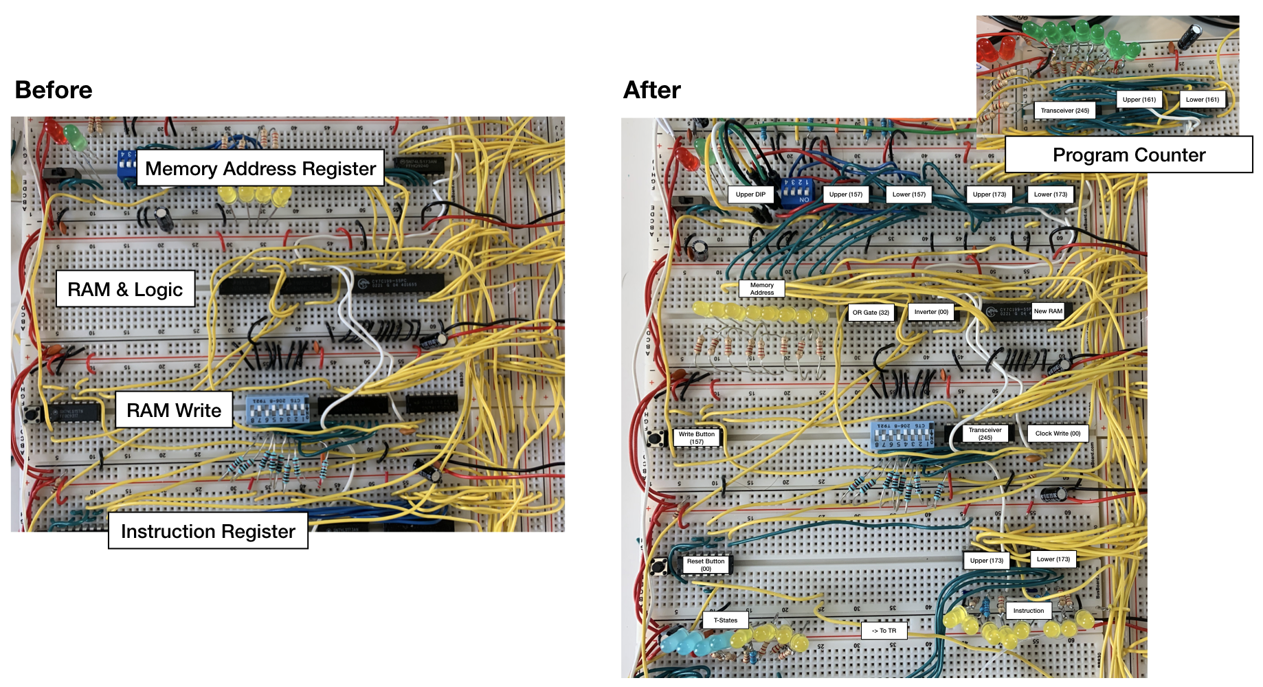
The RAM is expanded but it won’t actually do anything differently until we can give it more address lines. To do that, we need to expand the program counter and address register.
Expanding the Program Counter
Let’s start with the program counter, which is really simple to expand.
- Add another 74LS161 chip next to the existing one. Connect power and ground.
- Connect the Clock, Load, and Clear lines between the two 161 chips so that they can be controlled identically.
- Connect the Ripple Carry output of the lower chip (the one on the right) to the Enable input of the higher chip (the one on the left).
- Connect the extra 4 input lines to the bottom of the 74LS245 transceiver and the 4 output lines to the top. Make sure you wire them correctly so that when the two 4-bit counters are combined side-by-side into 8 bits, the counting progresses naturally from right to left.
- Connect the extra 4 lines from the 74LS245 to the bus and add 4 more LEDs so you can see what’s going on.
If you’ve done everything correctly, you should now have an 8-bit counter. You can test it by disconnecting the control lines and manually enabling the counter.
Expanding the Memory Address Register
Expanding the program counter isn’t very useful until the address register can actually reach the new memory. Don’t worry, this part is really easy! Depending on how you laid it out, you may have to redo all the wiring or you can get by just adding things inline.
- Replace the 4-bit DIP switch with an 8-bit one. Alternatively, you can use two DIP switches or just jumper wires. Wire one side of the switch to ground in the same alternating pattern as Ben’s original design.
- Add a 74LS157 selector next to the existing one. Add power and ground. Wire it up to the corresponding DIP switches, just like with the original.
- Add a 74LS173 register next to the existing one. Add power, ground, and tie M/N to ground. Tie the clock, enable (G1/G2), and reset lines between the two 173s together.
- Connect the upper half of the bus to the inputs of the new 173 register.
- Connect the outputs of the new 173 to the new 157.
- Add 4 LEDs with resistors to the left of the existing ones (or move the entire set of LEDs elsewhere) and wire them to the new 157 outputs.
- Wire the new 157 outputs to A4 - A7 on the RAM. No1te that A4 is on the top and the rest are on the bottom.
If everything has been hooked up correctly, you can ensure things are working well by going into program mode and using the new upper bits or going into run mode and making the counter count to a high value and make sure it’s reflected in the address register.
Adjusting the Instruction Register
The instruction register already holds 8 bits, but we can no longer represent both the opcode and the address in 8 bits. We’ll make the instruction register only hold opcodes and we’ll send the address separately. This means the current wiring is off and the LEDs are different colors, so we need to fix that.
- Remove the 74LS245 transceiver because it’s not needed. The instruction register never needs to output anything.
- If you want, replace the multiple colors of LEDs with a single color.
- Wire the ROM address lines to the outputs of the lower register. In Ben’s 4-bit design, the upper register contains the opcode. In the new 8-bit design, both registers contain the opcode but we’ll only use the lower part of the byte.
Now, you may be wondering why we’re still only connecting the 4 bits to the ROM when we have 8 bits for the opcode. If you recall in Ben’s design, the address lines need to signal three things: opcode, step, and flags. There are two unused address lines left, which you can use in three different ways:
- Extra flags (e.g., negative flag)
- Extra steps (16 vs. 8)
- Extra instructions (32 vs. 16)
In the future I’ll probably rework this to get added flexibility, but I chose to keep it simple for now and just stick to the original design.
Adjusting the Step Counter
There is one last bit to take care of before we program the ROM. Since we’re sending our addresses separately, each instruction will take extra steps and we need to make sure we don’t reset the counter too early. Since we no longer have an IO signal, we can use that as a dynamic reset signal and do away with the static reset altogether.
- Remove the reset line going from the 74LS138 decoder to the reset circuit and instead connect what used to be the IO line (rename it to TR for “T-State Reset”).
- Add more LEDs to the 74LS138 so you can see all 8 steps.
Testing!
At this stage, hopefully you’ve seen that every individual piece is working as expected. However, we can’t test anything end-to-end until we get the ROM updated, since the instructions make no sense.
Step 3: Update the Instruction Set
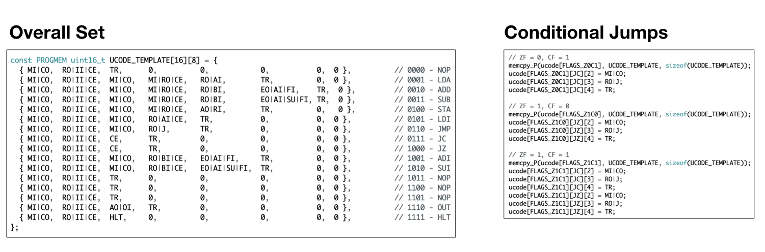
The instruction set requires only a few minimal modifications. Let’s go through them:
- Rename the
#define IOto#define TR - Add a step to each instruction that just has
TR. This will reset the counter early and eliminate empty steps. For example, yourNOPnow becomesMI|CO, RO|II|CE, TR, 0. - Let’s deal with non-jump instructions first.
MI|COandRO|II|CEstay the same because we always need to fetch the opcode. Before, we hadIO|MIsince the instruction register’s lower 4 bits contained the address. We just need to replace this with two steps:CO|MIandMI|RO|CE. These will fetch the address from the next byte instead and increment the program counter accordingly. - What about
LDI? You just need to addMI|COand then replaceIO|AIwithRO|AI|CE.LDIbecomes more useful because now you can enter a number from 0 to 255 directly. In fact, I also created immediate versions ofADDandSUBbecause it was so handy. HLT,OUT, andNOPdon’t need to use up more steps since there’s no data to pass them. Just remember that when you calculate locations for jumps, sometimes you need to count by 2 and other times only 1!- The
JMPinstruction is straightforward. Instead ofIO|Jyou need to use up another step and doMI|CO, RO|J. Notice that unlike the other instructions we don’t need to increment the counter a second time since we’re jumping anyway. - The condition jumps are only slightly trickier. The first thing is to look at the template. We need to have all branches of the instruction take up two bytes/steps even if we don’t jump, otherwise the computer will think the jump address is the next instruction. Before the
TRstep you added earlier, add another step toJCandJZthat just increments the counter (CE). - Now we need to take care of the conditions. You need to expand the one line into three that mimic the
JMPcommand. For example, for the case where zero flag = 0, carry flag = 1 you’d write:ucode[FLAGS_Z0C1][JC][2] = MI|CO; ucode[FLAGS_Z0C1][JC][3] = RO|J; ucode[FLAGS_Z0C1][JC][4] = TR;
Conclusion
And that’s it! You now have a fully 8-bit CPU that’s able to access 256 bytes of RAM and has some more efficient IPC to boot.
I originally published this as a Reddit post.