In this tutorial, I’ll explain how to enable the 8-bit CPU to support more traditional programming with subroutines and assembly, dramatically increasing its capabilities. I go through adding a stack pointer and stack with 74LS193 counters, interfacing with an Arduino to stand up an assembly toolchain, and add more control lines by using 74LS138 decoders instead of more ROMs. As a bonus, I also enable B register output and add a Schmitt trigger to clean up the clock signal.
This is the second part of a two-part series. You’ll need to have done the work in part one where I expanded the RAM and make it a full 8-bit CPU before following this tutorial.
Parts List
To only update the hardware, you’ll need:
- 2x 74LS138 (Datasheet, Jameco) which are decoders used to expand the control lines. You can reuse one from the step counter if you don’t mind reading binary numbers vs. an LED for each step.
- 1x 74LS04 (Datasheet, Jameco) which is an inverter to help expand the control lines.
- 2x 74LS193 (Datasheet, Jameco) which is a 4-bit up/down counter used to create the stack pointer.
- 1x 74LS245 (Datasheet, Jameco) which is a bus transceiver. You may have a spare one if you did my previous build.
- 1x 74LS00 (Datasheet, Jameco) which is a NAND gate to control the stack pointer.
- 8x Green LED, 1x Yellow LED, 4x Blue LEDs, 13x 220 Ohm resistors to display the stack pointer (green), the stack address (yellow), and the additional control lines (blue).
If you want to update the toolchain, you’ll need:
- Arduino Mega 2560 (Amazon) to create the programmer.
- Ribbon Jumper Cables (Amazon) to connect the Arduino to the breadboard.
- TL866 II Plus EEPROM Programmer (Amazon) to program the ROM.
Bonus Clock Improvement: One additional thing I did is replace the 74LS04 inverter in Ben’s clock circuit with a 74LS14 inverting Schmitt trigger (datasheet, Jameco). The pinouts are identical! Just drop it in, wire the existing lines, and then run the clock output through it twice (since it’s inverting) to get a squeaky clean clock signal. Useful if you want to go even faster with the CPU.
Step 1: Program with an Arduino and Assembler
There’s a certain delight in the physical programming of a computer with switches. This is how Bill Gates and Paul Allen famously programmed the Altair 8800 and started Microsoft. But at some point, the hardware becomes limited by how effectively you can input the software. After upgrading the RAM, I quickly felt constrained by how long it took to program everything.
You can continue to program the computer physically if you want and even after upgrading that option is still available, so this step is optional. There’s probably many ways to approach the programming, but this way felt simple and in the spirit of the build. We’ll use an Arduino Mega 2560, like the one in Ben’s 6502 build, to program the RAM. We’ll start with a homemade assembler then switch to something more robust.
Preparing the Physical Interface
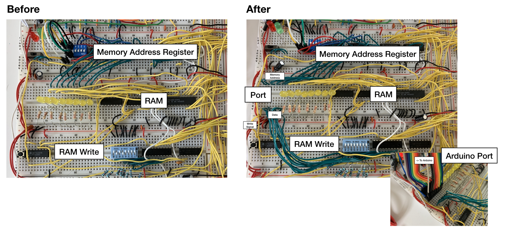
The first thing to do is prepare the CPU to be programmed by the Arduino. We already did the hard work on this in the RAM upgrade tutorial by using the bus to write to the RAM and disconnecting the control ROM while in program mode. Now we just need to route the appropriate lines to a convenient spot on the board to plug the Arduino into.
- This is optional, but I rewired all the DIP switches to have ground on one side, rather than alternating sides like Ben’s build. This just makes it easier to route wires.
- Wire the 8 address lines from the DIP switch, connecting the side opposite to ground (the one going to the chips) to a convenient point on the board. I put them on the far left, next to the address LEDs and above the write button circuit.
- Wire the 8 data lines from the DIP switch, connecting the side opposite to ground (the one going to the chips) directly below the address lines. Make sure they’re separated by the gutter so they’re not connected.
- Wire a line from the write button to your input area. You want to connect the side of the button that’s not connected to ground (the one going to the chip).
So now you have one convenient spot with 8 address lines, 8 data lines, and a write line. If you want to get fancy, you can wire them into some kind of connector, but I found that ribbon jumper cables work nicely and keep things tidy.
The way we’ll program the RAM is to enter program mode and set all the DIP switches to the high position (e.g., 11111111). Since the switches are upside-down, this means they’ll all be disconnected and not driving to ground. The address and write lines will simply be floating and the data lines will be weakly pulled up by 1k resistors. Either way, the Arduino can now drive the signals going into the chips using its outputs.
Creating the Arduino Programmer
Now that we can interface with an Arduino, we need to write some software. If you follow Ben’s 6502 video, you’ll have all the knowledge you need to get this working. If you want some hints and code, see below (source code):
- Create arrays for your data and address lines. For example:
const char ADDRESS_LINES[] = {39, 41, 43, 45, 47, 49, 51, 53};. Create your write line with#define RAM_WRITE 3. - Create functions to enable and disable your address and data lines. You want to enable them before writing. Make sure to disable them afterward so that you can still manually program using DIP switches without disconnecting the Arduino. The code looks like this (just change INPUT to OUTPUT accordingly):
for(int n = 0; n < 8; n += 1) { pinMode(ADDRESS_LINES[n], OUTPUT); } - Create a function to write to an address. It’ll look like
void writeData(byte writeAddress, byte writeData)and basically use two loops, one for address and one for data, followed by toggling the write. - Create a char array that contains your program and data. You can use
#defineto create opcodes like#define LDA 0x01. - In your main function, loop through the program array and send it through
writeData.
With this setup, you can now load multi-line programs in a fraction of a second! This can really come in handy with debugging by stress testing your CPU with software. Make sure to test your setup with existing programs you know run reliably. Now that you have your basic setup working, you can add 8 additional lines to read the bus and expand the program to let you read memory locations or even monitor the running of your CPU.
Making an Assembler
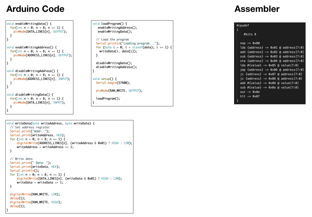
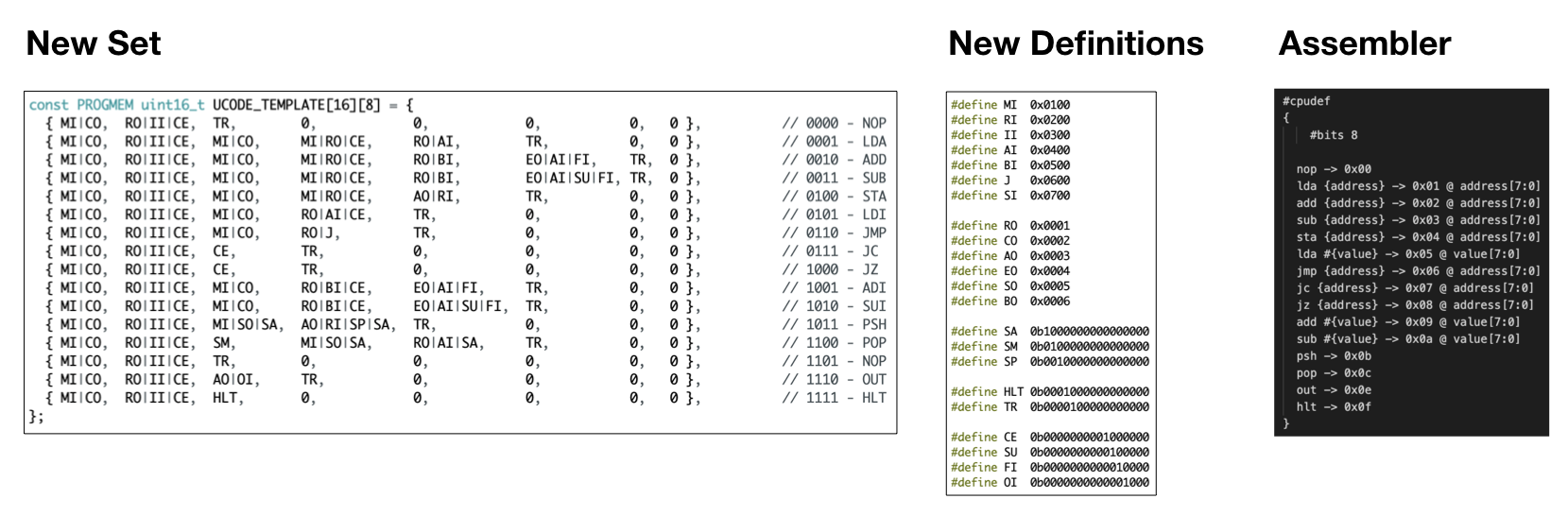
The above will serve us well but it’s missing a key feature: labels. Labels are invaluable in assembly because they’re so versatile. Jumps, subroutines, variables all use labels. The problem is that labels require parsing. Parsing is a fun project on the road to a compiler but not something I wanted to delve into right now—if you’re interested, you can learn about Flex and Bison. Instead, I found a custom assembler that lets you define your CPU’s instruction set and it’ll do everything else for you. Let’s get it setup:
- If you’re on Windows, you can use the pre-built binaries. Otherwise, you’ll need to install Rust and compile via
cargo build. - Create a file called
8bit.cpuand define your CPU instructions (source code). For example, LDA would belda {address} -> 0x01 @ address[7:0]. What’s cool is you can also now create the instruction’s immediate variant instead of having to call it LDI:lda #{value} -> 0x05 @ value[7:0]. - You can now write assembly by adding
#include "8bit.cpu"to the top of your code. There’s a lot of neat features so make sure to read the documentation! - Once you’ve written some assembly, you can generate the machine code using
./customasm yourprogram.s -f hexc -p. This prints out a char array just like our Arduino program used! - Copy the char array into your Arduino program and send it to your CPU.
At this stage, you can start creating some pretty complex programs with ease. I would definitely play around with writing some larger programs. I actually found a bug in my hardware that was hidden for a while because my programs were never very complex!
Step 2: Expand the Control Lines
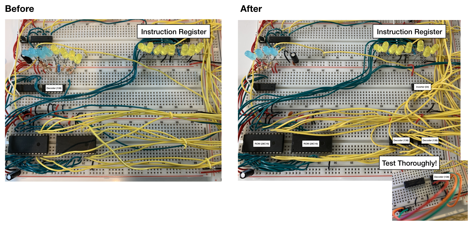
Before we can expand the CPU any further, we have to address the fact we’re running out of control lines. An easy way to do this is to add a 3rd 28C16 ROM and be on your way. If you want something a little more involved but satisfying, read on.
Right now the control lines are one hot encoded. This means that if you have 4 lines, you can encode 4 states. But we know that a 4-bit binary number can encode 16 states. We’ll use this principle via 74LS138 decoders, just like Ben used for the step counter.
Choosing the Control Line Combinations
Everything comes with trade-offs. In the case of combining control lines, it means the two control lines we choose to combine can never be activated at the same time. We can ensure this by encoding all the inputs together in the first 74LS138 and all the outputs together in a second 74LS138. We’ll keep the remaining control lines directly connected.
Rewiring the Control Lines
If your build is anything like mine, the control lines are a bit of a mess. You’ll need to be careful when rewiring to ensure it all comes back together correctly. Let’s get to it:
- Place the two 74LS138 decoders on the far right side of the breadboard with the ROMs. Connect them to power and ground.
- You’ll likely run out of inverters, so place a 74LS04 on the breadboard above your decoders. Connect it to power and ground.
- Carefully take your inputs (
MI, RI, II, AI, BI, J) and wire them to the outputs of the left 74LS138. Do not wire anything to O0 because that’s activated by 000 which won’t work for us! - Carefully take your outputs (
RO, CO, AO, EO) and wire them to the outputs of the right 74LS138. Remember, do not wire anything to O0! - Now, the 74LS138 outputs are active low, but the ROM outputs were active high. This means you need to swap the wiring on all your existing 74LS04 inverters for the LEDs and control lines to work. Make sure you track which control lines are supposed to be active high vs. active low!
- Wire E3 to power and E2 to ground. Connect the E1 on both 138s together, then connect it to the same line as OE on your ROMs. This will ensure that the outputs are disabled when you’re in program mode. You can actually take off the 1k pull-up resistors from the previous tutorial at this stage, because the 138s actively drive the lines going to the 74LS04 inverters rather than floating like the ROMs.
At this point, you really need to ensure that the massive rewiring job was successful. Connect 3 jumper wires to A0-A2 and test all the combinations manually. Make sure the correct LED lights up and check with a multimeter/oscilloscope that you’re getting the right signal at each chip. Catching mistakes at this point will save you a lot of headaches! Now that everything is working, let’s finish up:
- Connect A0-A2 of the left 74LS138 to the left ROM’s A0-A2.
- Connect A0-A2 of the right 74LS138 to the right ROM’s A0-A2.
- Distribute the rest of the control signals across the two ROMs.
Changing the ROM Code
This part is easy. We just need to update all of our #define with the new addresses and program the ROMs again. For clarity that we’re not using one-hot encoding anymore, I recommend using hex instead of binary. So instead of #define MI 0b0000000100000000, we can use #define MI 0x0100, #define RI 0x0200, and so on.
Testing
Expanding the control lines required physically rewiring a lot of critical stuff, so small mistakes can creep up and make mysterious errors down the road. Write a program that activates each control line at least once and make sure it works properly! With your assembler and Arduino programmer, this should be trivial.
Bonus: Adding B Register Output
With the additional control lines, don’t forget you can now add a BO signal easily which lets you fully use the B register.
Step 3: Add a Stack
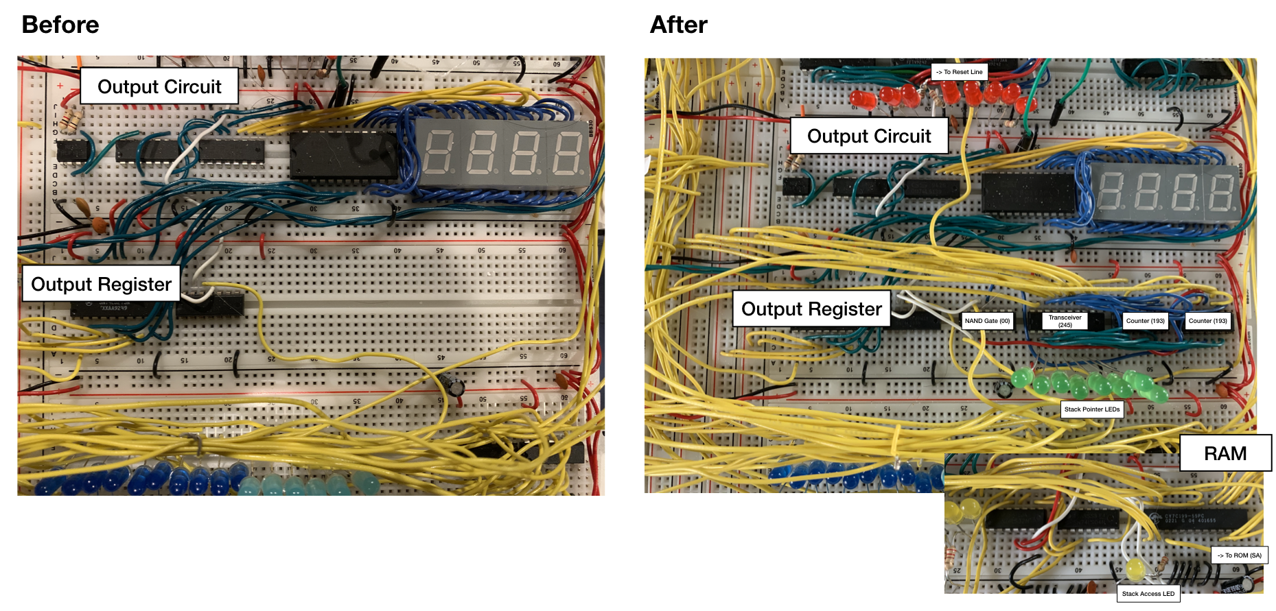
Adding a stack significantly expands the capability of the CPU. It enables subroutines, recursion, and handling interrupts (with some additional logic). We’ll create our stack with an 8-bit stack pointer hard-coded from $0100 to $01FF, just like the 6502.
Wiring up the Stack Pointer
A stack pointer is conceptually similar to a program counter. It stores an address, you can read it and write to it, and it increments. The only difference between a stack pointer and a program counter is that the stack pointer must also decrement. To create our stack pointer, we’ll use two 74LS193 4-bit up/down binary counters:
- Place a 74LS00 NAND gate, 74LS245 transceiver, and two 74LS193 counters in a row next to your output register. Wire up power and ground.
- Wire the the Carry output of the right 193 to the Count Up input of the left 193. Do the same for the Borrow output and Count Down input.
- Connect the Clear input between the two 193s and with an active high reset line. The B register has one you can use on its 74LS173s.
- Connect the Load input between the two 193s and to a new active low control line called
SIon your 74LS138 decoder. - Connect the QA-QD outputs of the lower counter to A8-A5 and the upper counter to A4-A1. Pay special attention because the output are in a weird order (BACD) and you want to make sure the lower A is connected to A8 and the upper A is connected to A4.
- Connect the A-D inputs of the lower counter to B8-B5 and the upper counter to B4-B1. Again, the inputs are in a weird order and on both sides of the chip so pay special attention.
- Connect the B1-B8 outputs of the 74LS245 transceiver to the bus.
- On the 74LS245 transceiver, connect DIR to power (high) and connect OE to a new active low control line called
SOon your 74LS138 decoder. - Add 8 LEDs and resistors to the lower part of the 74LS245 transceiver (A1-A8) so you can see what’s going on with the stack pointer.
Enabling Increment & Decrement
We’ve now connected everything but the Count Up and Count Down inputs. The way the 74LS193 works is that if nothing is counting, both inputs are high. If you want to increment, you keep Count Down high and pulse Count Up. To decrement, you do the opposite. We’ll use a 74LS00 NAND gate for this:
- Take the clock from the 74LS08 AND gate and make it an input into two different NAND gates on the 74LS00.
- Take the output from one NAND gate and wire it to the Count Up input on the lower 74LS193 counter. Take the other output and wire it to the Count Down input.
- Wire up a new active high control line called
SPfrom your ROM to the NAND gate going into Count Up. - Wire up a new active high control line called
SMfrom your ROM to the NAND gate going into Count Down.
At this point, everything should be working. Your counter should be able to reset, input a value, output a value, and increment/decrement. But the issue is it’ll be writing to $0000 to $00FF in the RAM! Let’s fix that.
Accessing Higher Memory Addresses
We need the stack to be in a different place in memory than our regular program. The problem is, we only have an 8-bit bus, so how do we tell the RAM we want a higher address? We’ll use a special control line to do this:
- Wire up an active high line called
SAfrom the 28C16 ROM to A8 on the Cypress CY7C199 RAM. - Add an LED and resistor so you can see when the stack is active.
That’s it! Now, whenever we need the stack we can use a combination of the control line and stack pointer to access $0100 to $01FF.
Updating the Instruction Set
All that’s left now is to create some instructions that utilize the stack. We’ll need to settle some conventions before we begin:
- Empty vs. Full Stack: In our design, the stack pointer points to the next empty slot in memory, just like on the 6502. This is called an “empty stack” convention. ARM processors use a “full stack” convention where the stack points to the last filled slot.
- Ascending vs. Descending Stack: In our design, the stack pointer increases when you add something and decreases when you remove something. This is an “ascending stack” convention. Most processors use a “descending stack”, so we’re bucking the trend here.
If you want to add a little personal flair to your design, you can change the convention fairly easily. Let’s implement push and pop (source code):
- Define all your new control lines, such as
#define SI 0x0700and#define SO 0x0005. - Create two new instructions:
PSH(1011) andPOP(1100). PSHstarts the same as any other for the first two steps:MI|COandRO|II|CE. The next step is to put the contents of the stack pointer into the address register viaMI|SO|SA. Recall thatSAis the special control line that tells the memory to access the$01XXbank rather than$00XX.- We then take the contents of
AOand write it into the RAM. We can also increment the stack pointer at this stage. All of this is done via:AO|RI|SP|SA, followed byTR. POPis pretty similar. Start off withMI|COandRO|II|CE. We then need to take a cycle and decrement the stack pointer withSM. Like withPSH, we then set the address register withMI|SO|SA.- We now just need to output the RAM into our A register with
RO|AI|SAand then end the instruction withTR. - Updating the assembler is easy since neither instruction has operands. For example, push is just
psh -> 0x0B.
And that’s it! Write some programs that take advantage of your new 256 byte stack to make sure everything works as expected.
Step 4: Add Subroutine Instructions
The last step to complete our stack is to add subroutine instructions. This allows us to write complex programs and paves the way for things like interrupt handling.
Subroutines are like a blend of push/pop instructions and a jump. Basically, when you want to call a subroutine, you save your spot in the program by pushing the program counter onto the stack, then jumping to the subroutine’s location in memory. When you’re done with the subroutine, you simply pop the program counter value from the stack and jump back into it.
We’ll follow 6502 conventions and only save and restore the program counter for subroutines. Other CPUs may choose to save more state, but it’s generally left up to the programmer to ensure they’re not wiping out states in their subroutines (e.g., push the A register at the start of your subroutine if you’re messing with it and restore it before you leave).
Adding an Extra Opcode Line
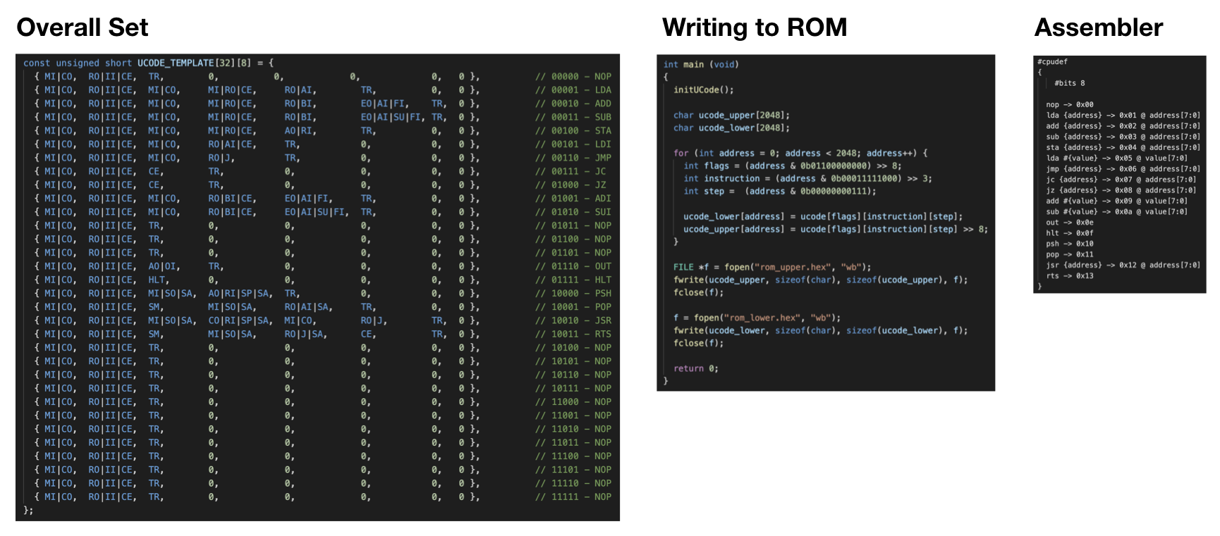
I’ve started running low on opcodes at this point. Luckily, we still have two free address lines we can use. To enable 5-bit opcodes, simply wire up the 4Q output of your upper 74LS173 register to A7 of your 28C16 ROM (this assumes your opcodes are at A3-A6).
Updating the ROM Writer
At this point, you simply need to update the Arduino writer to support 32 instructions vs. the current 16. So, for example, UCODE_TEMPLATE[16][8] becomes UCODE_TEMPLATE[32][8] and you fill in the 16 new array elements with nop. The problem is that the Arduino only has so much memory and with the way Ben’s code is written to support conditional jumps, it starts to get tight.
I bet the code can be re-written to handle this, but I had a TL866II Plus EEPROM programmer handy from the 6502 build and I felt it would be easier to start using that instead. Converting to a regular C program is really simple (source code):
- Copy all the
#define, globalconstarrays (don’t forget to expand them from 16 to 32), andvoid initUCode(). Add#include <stdio.h>and#include <string.h>to the top. - In your traditional
int main (void)C function, after initializing withinitUCode(), make two arrays:char ucode_upper[2048]andchar ucode_lower[2048]. - Take your existing loop code that loops through all addresses:
for (int address = 0; address < 2048; address++). - Modify instruction to be 5-bit with
int instruction = (address & 0b00011111000) >> 3;. - When writing, just write to the arrays like so:
ucode_lower[address] = ucode[flags][instruction][step];anducode_upper[address] = ucode[flags][instruction][step] >> 8;. - Open a new file with
FILE *f = fopen("rom_upper.hex", "wb");, write to it withfwrite(ucode_upper, sizeof(char), sizeof(ucode_upper), f);and close it withfclose(f);. Repeat this with the lower ROM too. - Compile your code using gcc (you can use any C compiler), like so:
gcc -Wall makerom.c -o makerom.
Running your program will spit out two binary files with the full contents of each ROM. Writing the file via the TL866II Plus requires minipro and the following command: minipro -p CAT28C16A -w rom_upper.hex.
Adding Subroutine Instructions
At this point, I cleaned up my instruction set layout a bit. I made psh and pop 1000 and 1001, respectively. I then created two new instructions: jsr and rts. These allow us to jump to a subroutine and returns from a subroutine. They’re relatively simple:
- For
jsr, the first three steps are the same aspsh:MI|CO,RO|II|CE,MI|SO|SA. - On the next step, instead of
AOwe useCOto save the program counter to the stack:CO|RI|SP|SA. - We then essentially read the 2nd byte to do a jump and terminate:
MI|CO,RO|J. - For
rts, the first four steps are the same aspop:MI|CO,RO|II|CE,SM,MI|SO|SA. - On the next step, instead of
AIwe useJto load the program counter with the contents in stack:RO|J|SA. - We’re not done! If we just left this as-is, we’d jump to the 2nd byte of
jsrwhich is not an opcode, but a memory address. All hell would break loose! We need to add aCEstep to increment the program counter and then terminate.
Once you update the ROM, you should have fully functioning subroutines with 5-bit opcodes. One great way to test them is to create a recursive program to calculate something—just don’t go too deep or you’ll end up with a stack overflow!
Conclusion
And that’s it! Another successful upgrade of your 8-bit CPU. You now have a very capable machine and toolchain. At this point I would have a bunch of fun with the software aspects. In terms of hardware, there’s a number of ways to go from here:
- Interrupts. Interrupts are just special subroutines triggered by an external line. You can make one similar to how Ben did conditional jumps. The only added complexity is the need to load/save the flags register since an interrupt can happen at any time and you don’t want to destroy the state. Given this would take more than 8 steps, you’d also need to add another line for the step counter (see below).
- ROM expansion. At this point, address lines on the ROM are getting tight which limits any expansion possibilities. With the new approach to ROM programming, it’s trivial to switch out the 28C16 for the 28C256 that Ben uses in the 6502. These give you 4 additional address lines for flags/interrupts, opcodes, and steps.
- LCD output. At this point, adding a 16x2 character LCD like Ben uses in the 6502 is very possible.
- Segment/bank register. It’s essentially a 2nd memory address register that lets you access 256-byte segments/banks of RAM using bank switching. This lets you take full advantage of the 32K of RAM in the Cypress chip.
- Fast increment instructions. Add these to registers by replacing 74LS173s with 74LS193s, allowing you to more quickly increment without going through the ALU. This is used to speed up loops and array operations.
I originally published this as a Reddit post.